Modern System-on-Chips (SoCs) include security critical features which are often configured securely using One-Time Programmable (OTP) bits, often implemented using electronic fuses (i.e., eFuses). Most SoCs will transfer these configuration bits from OTP memory to dedicated shadow registers from where they will be consumed by either hardware modules (e.g. cryptographic engines) or software (e.g. ROM code). These bits must be transferred correctly during boot to ensure the SoC is configured as intended. This mechanism is referred to by us in the remainder of this blog post as the OTP Data Transfer or simply the OTP Transfer. When the OTP Transfer is completed, the SoC is assumed to operate as expected, according to the supplied (security) configuration. However, what if we can break this fundamental assumption?
Fault Injection (FI) attacks have become increasingly popular as a means of breaking into devices, such as consoles, especially when no software vulnerabilities have yet been identified. These attacks are typically used to manipulate software control flow, but they can also impact the intended behavior of functionality implemented purely in hardware, including the OTP Transfer.
During our presentation at Blue Hat IL 2019, we introduced the concept of glitching the OTP Data Transfer of modern chips. At that time, we did not focus on any particular target. However, since then, LimitedResults glitched the OTP transfer of the ESP32 using Voltage Fault Injection in order to extract the Secure Boot and Flash Encryption keys. To further explore this technique, we decided to apply Electromagnetic Fault Injection (EMFI), which offers several notable advantages.
In this blog post, we describe how we were able to successfully execute an EMFI attack on the OTP transfer process of the ESP32 using commercially available tooling. We presented this work at hardwear.io USA 2022.
It’s important to point out, we performed this attack on the original ESP32, we did not test any other ESP32 chip. Espressif actually updated the security architecture of the original ESP32, resulting in the ESP32-V3, which is hardened against Fault Injection attacks. Espressif released two advisories (CVE-2019-15894 and CVE-2019-17391) providing more details about the changes. Interestingly, in line with this Espressif’s advisories, Ledger’s researchers found that the ESP32-V3 is indeed hardened against Fault Injection attacks. You can find more information on this in their presentation or paper).
OTP Memory
Let’s take a moment to discuss OTP memory. Most chips, notably SoCs, include OTP memory, which is used to store configuration bits and cryptographic material, such as keys. There are a variety of different technologies that can be used to implement OTP memory (e.g. eFuse, Anti-fuse, Floating gate-based, etc.). From a conceptual point of view, they typically share at least one characteristic, once a bit is set to one (1), it cannot be set to zero (0) any more. This means, once a security feature is enabled using a dedicated OTP bit, it cannot be disabled any more.
The data from OTP memory is typically not directly consumed (i.e., read) from OTP memory. There’s often a dedicated OTP controller implemented around the OTP PHY in order to read and write to the OTP memory. Depending on the chip the bits may be transferred to intermediate shadow registers or directly to the register of the destination IP. These intermediate transfers are often done early during boot, as the values configure security critical features, such as Secure Boot.
Some of the data may be actually accessible by the CPU, which often means the shadow registers containing such information are memory mapped. A diagram visualizing a potential OTP memory design of a chip is shown below.
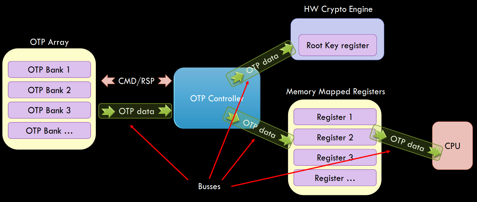
The above design is potentially vulnerable to several Fault Injection attacks. For example, an attacker can inject a glitch when the OTP PHY is read, OTP memory is transfer and OTP memory is stored. Then, each time the hardware of CPU accesses these bits, whether from dedicated or shadow registers, an attacker can glitch it again. This shows the important of data integrity at the moment of transfer and moment of rest. If such integrity is not assured adequately, it provides an attacker an opportunity, one of which is described in this blog post.
Target
During this research we targeted the original ESP32 in a 6mm x 6mm package (i.e., D0WDQ6) as is shown below.
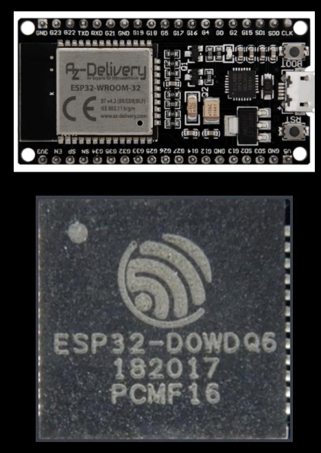
The chip itself is housed on a DevKitC development board which are publicly available.
Test application
We programmed a bootloader that prints the entire OTP memory from shadow registers as is shown in the snippet below for block 0 (i.e., 28 bytes in total).
...
uint32_t block0[7] = { 0 };

block0[0] = *(uint32_t *)(0x3FF5A000);
block0[1] = *(uint32_t *)(0x3FF5A004);
block0[2] = *(uint32_t *)(0x3FF5A008);
block0[3] = *(uint32_t *)(0x3FF5A00C);
block0[4] = *(uint32_t *)(0x3FF5A010);
block0[5] = *(uint32_t *)(0x3FF5A014);
block0[6] = *(uint32_t *)(0x3FF5A018);
...
The expected output (i.e., no glitch) of this test application is shown below.
+ Block 0: 00020100 a3d2c1e0 0001c8c9 0000a000 00000132 00000000 00000014 (expected)
Any change in the expected output is an indication were were successful in affecting the OTP transfer.
Setup
We used Riscure’s EM-FI Transient Probe to inject EM glitches into the target’s circuitry. Riscure’s EM Probe Station allows us to move the EMFI Probe accross the chip’s surface.
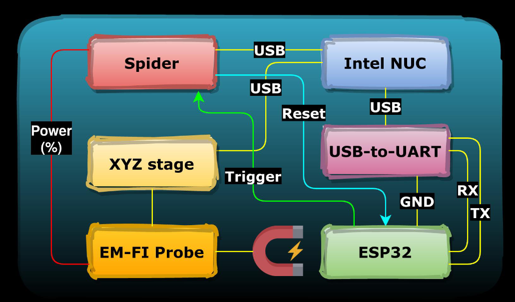

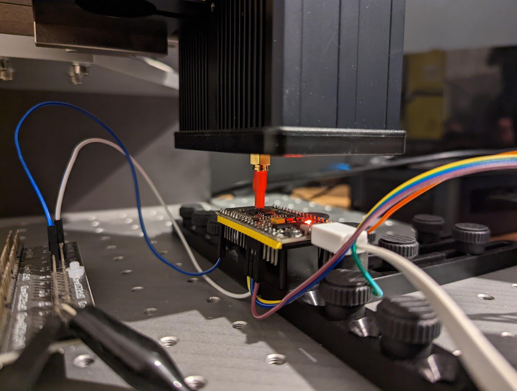
The advantages of injecting injecting EM glitches, compared to voltage glitches, is that the required target modifications are limited and that it’s possible to affect specific parts of the chip’s circuitry. On the other hand, there is a disadvantage as well, as it’s required to identify a vulnerable location where the OTP Transfer can be affected. However, using the Riscure setup, we were able to perform our experiments at different locations automatically.
Timing
The glitches are timed based of the reset signal. The attack window we used, is the time between reset and the time we observe the first activity on the flash lines. This yield an attack window of about 1.25 ms.
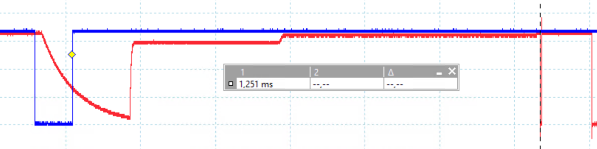
We decreased the attack window slightly by injecting only glitches before the first print on the UART interface is observed.
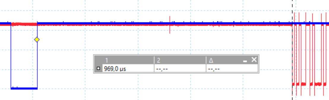
This yielded us an attack window of roughly 969 μs which we consider not too small and not too large.
Location
We scanned the entire surface of the chip in a 30x30 grid while injecting a glitches during boot. This means, for each experiment, we performed a reset of the chip.
We performed ~60,000 experiments of which a plot is shown below.


Interestingly, we observed 9 successful glitches for which the output is shown below.
+ Block 0: 00020100 a3d2c1e0 0001c8c9 0000a000 00000132 00000000 00000014 (no glitch)
- Block 0: 00020100 a3d2c1e0 0001c8c9 0000a000 00000132 00000000 00000014 (glitched)
- Block 0: 00020100 a3d2c1e0 0001c8c9 0000a000 00000132 00000000 00000014 (glitched)
These are actually located at four different locations as is shown below. We decided to fix the EM Probe at the location where we observed most of the successful glitches.

![]()
Fixing the EM Probe at a specific location decreases the glitch parameter search space. Of course, if a bad location is chosen, then it will be impossible to get a successful glitch. However, as we already observed successful glitches, we were confident that this would be the right move.
Exploration
We performed ~165,000 experiments with a glitch power randomized between 50% and 100%. The results of this glitch campaign are shown below.
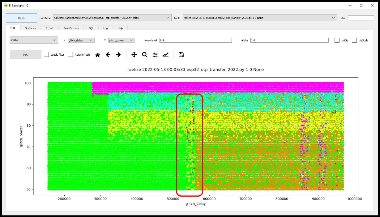
When we analyze the successful glitches, we see that we are able to perform bit-level corruptions inside the data stored in the shadow registers as is shown below.
+ Block 0: 00020100 a3d2c1e0 0001c8c9 0000a000 00000132 00000000 00000014 (no glitch)
- Block 0: 00000100 a3d2c1e0 0001c8c9 0000a000 00000132 00000000 00000014 (glitched)
- Block 0: 00020100 a3d2c0e0 0001c8c9 0000a000 00000132 00000000 00000014 (glitched)
- Block 0: 00020100 a3d2c1e0 0001c889 0000a000 00000132 00000000 00000014 (glitched)
- Block 0: 00020100 a3d2c1e0 0001c8c9 0000a000 00000032 00000000 00000014 (glitched)
- Block 0: 00020100 a3d2c1e0 0001c8c9 0000a000 00000132 00000000 00000004 (glitched)
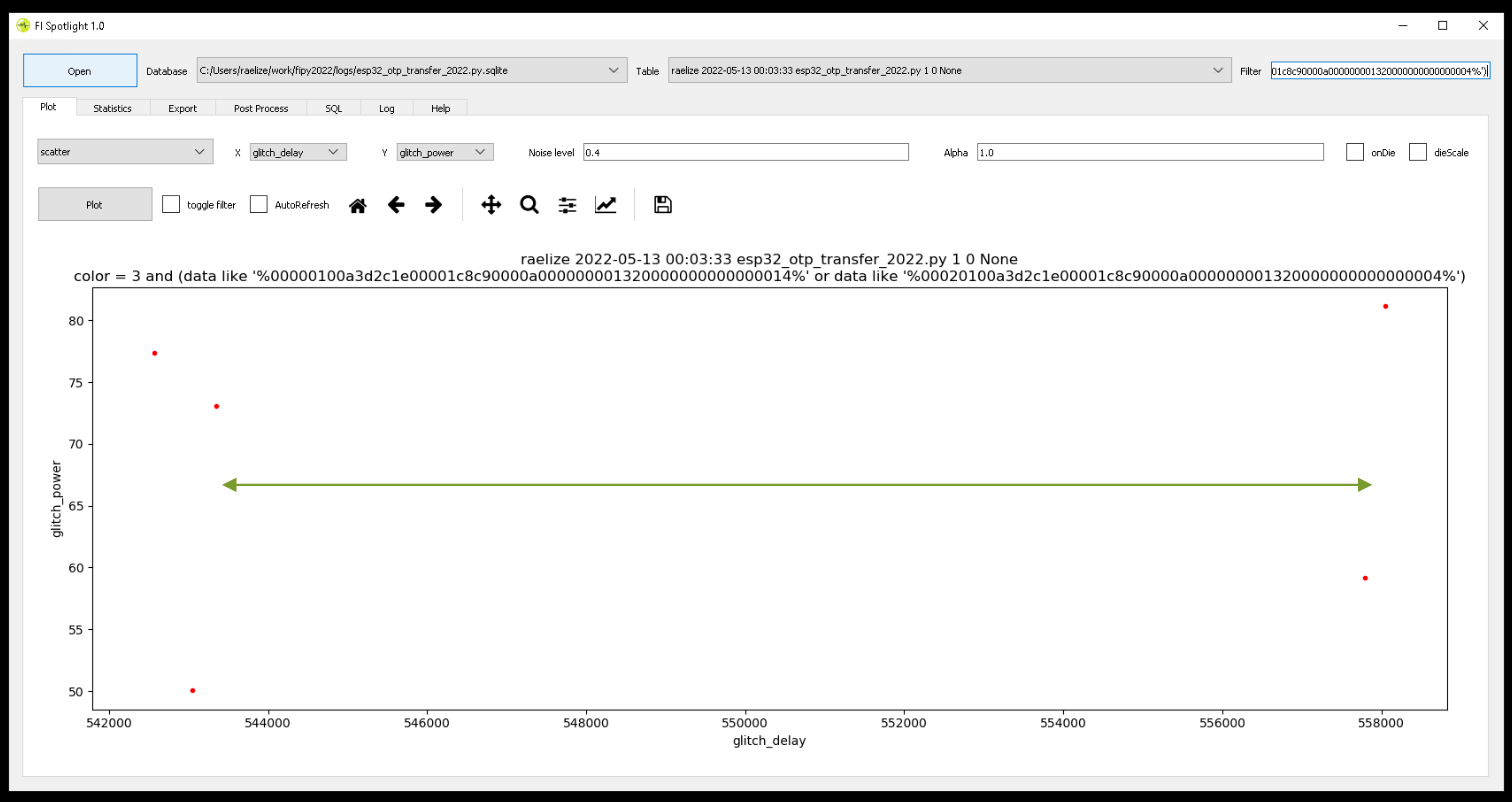
When we analyze the area where we observe the successful glitches, we see that there are specific moments in time where we are able to affect the data stored in the shadow registers.

As expected, as it’s likely that the OTP memory is copied into the shadow registers sequentially, we will need to glitch earlier if we want to corrupt a bit at the start of block 0 and later when we want to corrupt a bit at the end. This timing dependency is visualized in the plot below.
+ Block 0: 00020100 a3d2c1e0 0001c8c9 0000a000 00000132 00000000 00000014 (no glitch)
- Block 0: 00000100 a3d2c1e0 0001c8c9 0000a000 00000132 00000000 00000014 (glitched; early)
- Block 0: 00020100 a3d2c1e0 0001c8c9 0000a000 00000132 00000000 00000004 (glitched; late)
To conclude our analysis, using an EM glitch, we are able to affect the OTP Data Transfer, at the bit-level, which may allow us to disable security critical features like Secure Boot. At this point in time, we do not know if all the (security) features actually consume these modified bits. In principle, they could be reading them from a completely different location (i.e., register). Therefore, we needed to perform the actual attacks in order to confirm that we are successful in disabling or reconfiguring security critical features.
Attack 1: Reading Secure Boot Key
One of the first attacks we performed is to read out the Secure Boot Key. This key is stored in the BLK2 region of the OTP memory and cannot be read as the read protection for this region should be enabled. Note, for this version of the ESP32 chip, the Secure Boot key is a symmetric key (i.e., shared secret). An attacker with access to this key is able to sign arbitrary payloads (e.g., bootloader).
We prepared the target by setting the following fuses:
ABS_DONE0for enabling Secure BootSECURE_BOOT_KEY(BLK2) for setting the Secure Boot keyRD_DIS_BLK2for enabling read protection of Secure Boot key
The goal is to modify the RD_DIS_BLK2 which will remove the read protection of the BLK2 region, which allows us to read out the Secure Boot key.
We programmed a correctly signed bootloader that prints all the fuses, this allowed us to identify a successful attack. Also, it allows us to identify if we glitch too early (i.e., we modify a bit before the read protection bit) and similarly when we are too late.
We performed 450,000 experiments, which resulted in 189 successful glitches where we were able to read out the Secure Boot key.

As you can see in the glitched output below, the read protection bit changed from 1 to 0 which allowed us to read out the Secure Boot key.
+ No Glitch
+ Block 0: 00020100 a3d2c1e0 0001c8c9 0000a000 00000132 00000000 00000014
+ Block 2: 00000000 00000000 00000000 00000000 00000000 00000000 00000000 00000000

- Successful Glitch
- Block 0: 00000100 a3d2c1e0 0001c8c9 0000a000 00000132 00000000 00000014
- Block 2: 570b8325 8df3b44a 8dbe92d8 934a7e19 b9e116d4 8c0b50fc ebe4b056 688860da
When we focus the glitch parameters around the region where we observe the successful glitches, we have a success rate of roughly 1%, which allows us to read out the Secure Boot key within minutes.
Attack 2: Bypass Secure Boot & Read Secure Boot Key
Of course, an attacker willing to extract the Secure Boot key, may also need to bypass Secure Boot itself. Therefore, we decided to test if it’s possible to modify two OTP configuration bits, one to disable Secure Boot and one to read out the Secure Boot key.
We prepared the target by setting the following fuses:
ABS_DONE0for enabling Secure BootSECURE_BOOT_KEY(BLK2) for setting the Secure Boot keyRD_DIS_BLK2for enabling read protection of Secure Boot key
The goals is to modify the ABS_DONE0 and RD_DIS_BLK2 bits in order to disable Secure Boot and remove the read protection of the BLK2 region, which allows us to read out the Secure Boot key.
We programmed an invalid bootloader that prints all the fuses, this allowed us to identify that we bypassed Secure Boot and that we modified the RD_DIS_BLK2 correctly.
As you can imagine, for this attack to succeed, we needed two glitches, one to changed RD_DIS_BLK2 and one to change ABS_DONE0. We timed the first glitch from reset and the second glitch from the moment in time we inject the first glitch.

When we focus the glitch parameters around the region where we observe the successful glitches, we have a success rate of roughly ~0.05%, which allows us to bypass Secure Boot and read out the Secure Boot key within a hour.
Attack 3: Bypass Flash Encryption, Bypass Secure Boot & Read Keys
Espressif recommends, besides Secure Boot, to also enable Flash Encryption. When this feature is enabled, the entire bootloader is encrypted, which prevents an attacker from making trivial modifications (e.g., to read out the fuses or the Secure Boot key).
We decided to devise a method for levaring the vulnerable OTP transfer in order to bypass Secure Boot, bypass Flash Encryption and read out both Secure Boot key and Flash Encryption key. We tried a few interesting things, but we failed to succeed.
Let’s try something else…
Attack 4: Bypass JTAG Protection
The ESP32 contains a hardware JTAG interface which can be used for a wide variety of purposes (e.g. RW memory, debug software, etc.). This interface allows an attacker to access the internals of the ESP32 and access the unencrypted flash. Therefore, there is a dedicated security feature to disable the JTAG interface, which is enabled with a dedicated OTP bit: DISABLE_JTAG. You probably already realize where this is going…
We prepared the target by setting the following fuses:
ABS_DONE0for enabling Secure BootSECURE_BOOT_KEY(BLK2) for setting the Secure Boot keyRD_DIS_BLK2for enabling read protection of Secure Boot keyFLASH_CRYPT_CNTfor enabling Flash EncryptionFLASH_ENCRYPTION_KEY(BLK1) for setting the Flash Encryption keyRD_DIS_BLK1for enabling read protection of Flash Encryption keyDISABLE_JTAGfor disabling the JTAG interface
Needless to say, the above configuration, the is the configuration that Espressif recommended for security sensitive devices.
The goal of this attack is to open the JTAG interface (i.e., unset DISABLE_JTAG) during the OTP Transfer. Then, with the opened JTAG, extract the plaintext firmware in order to bypass Flash Encryption. Once unlocked, the JTAG interface can also be used to execute arbitrary code (i.e., bypass Secure Boot).
We programmed a valid bootloader, but it’s no so relevant for this attack as we are aiming to affect hardware instead of software.
We performed 250,000 experiments, which resulted in 14 successful glitches where we were able to enable the JTAG interfaces in order to extract the unencrypted flash contents.
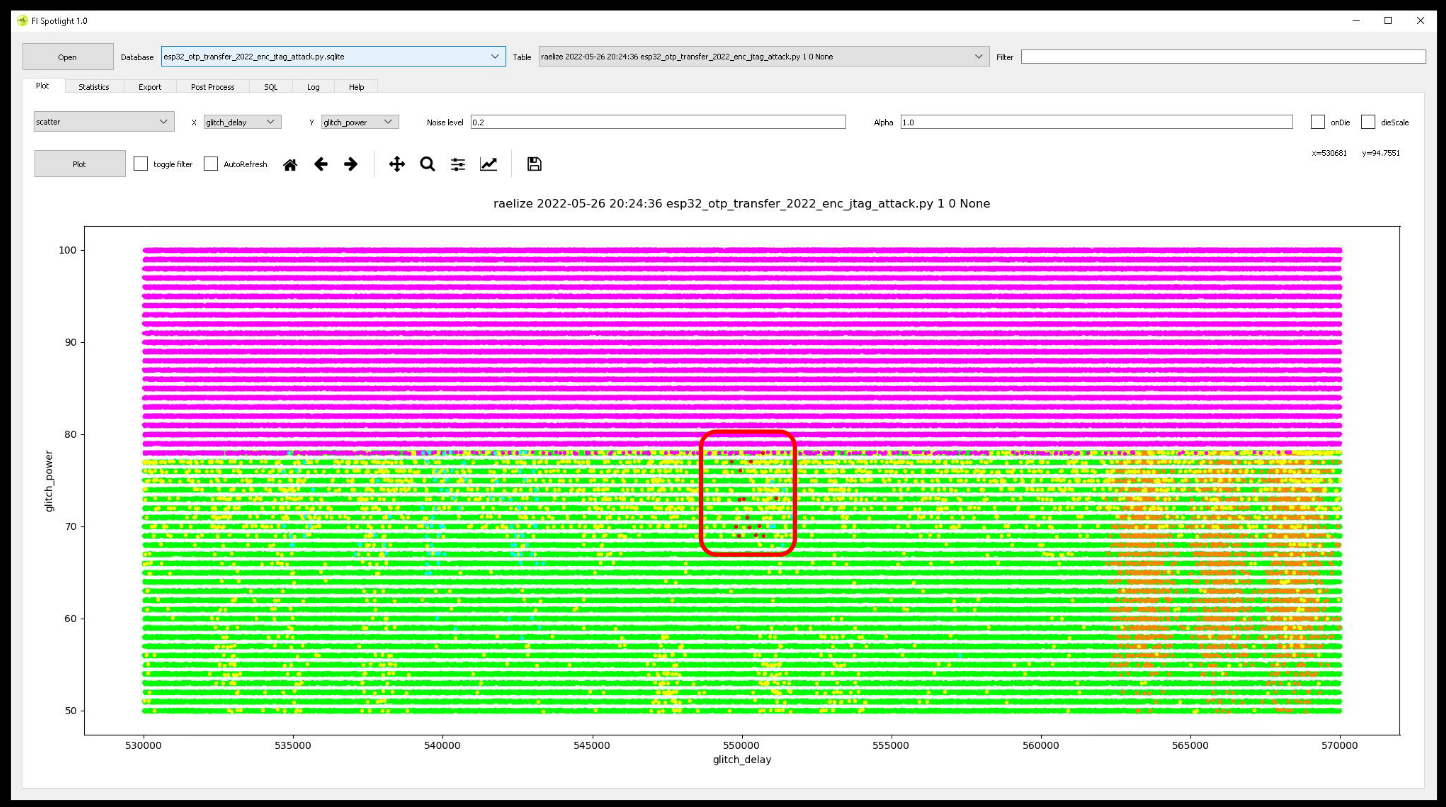
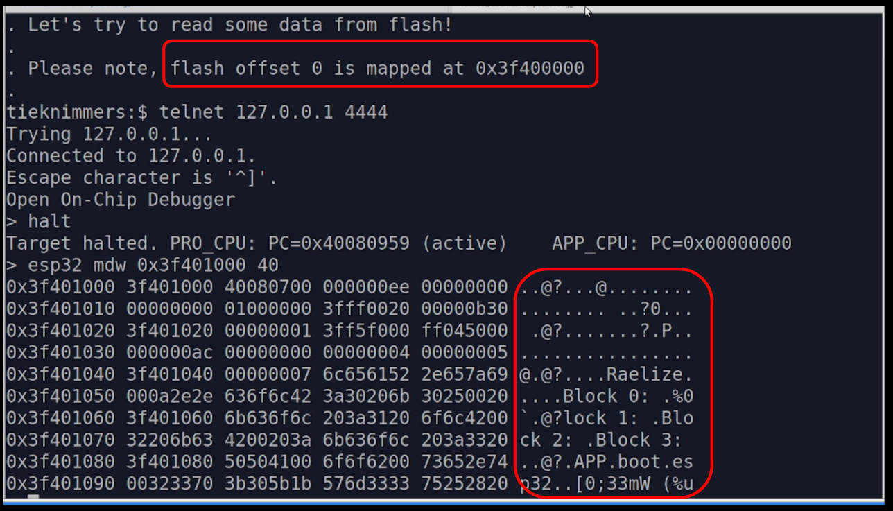
In the screenshot below we demonstrate reading out the unencrypted flash contents using the JTAG interface. We used a standard FT2232 from FTDI to interface with the JTAG interface using the OpenOCD software found in Espressif’s ESP-IDF.
When we focus the glitch parameters around the region where we observe the successful glitches, we have a success rate of roughly ~0.12%, which allows us to unlock the JTAG interface within a few minutes.
Final words
Using an EM glitch on the OTP transfer, we were successful in bypassing most of the security features of the original ESP32 chip. By enabling the JTAG interface, by modifying the OTP bit responsible for disabling it, we were able to bypass the Secure Boot and Flash Encryption, using a single glitch.
This type of attack is not specific for Espressif’s ESP32 chip and may be applicable chips made by other manufacturers as well. Espressif actually updated the security architecture of the original ESP32, resulting in the ESP32-V3, where the OTP transfer is hardened against Fault Injection attacks. Espressif released two advisories (#1 and #2) providing more details about the changes. Furthermore, for their Secure Boot v2 scheme, they use an asymmetric algorithm which requires no shared secret to be stored in OTP memory for assuring the integrity of the contents stored in external flash. Hence Secure Boot cannot be bypassed by extracting a secret from OTP memory.
Interestingly, research conducted by Ledger’s team has found that the ESP32-V3 seems to be hardened against the attack described in this blog post. You can find more information on this in their presentation or paper).
When Fault Injection attacks are considered by a chip’s threat model, the integrity of data, especially when transferred from one location to another, cannot be guaranteed any more. Therefore, in order to mitigate this attack, great care must be taken to assure the integrity of the (most) security critical data stored in OTP memory. This must be done at rest when the chip is off, at boot when the chip is starting and at runtime when the software is running.
Feel free to reach out for questions or remarks related to this research. As always, we are available to give training on the research we perform, during which you will gain hands-on experience exploiting the vulnerabilities described in this blog post.
- Raelize.